Digital Logic 2065
Long Answer Questions:
AI is thinking...
Attempt any TWO questions: (10x2=20)
AI is thinking...
1. Draw a block diagram, truth table and logic circuit of a 16 x 1 multiplexer and explain its working principle.
In 16 X 1 multiplexer:
Input lines 16 = 24 i.e. 4 Selection lines
Input lines will be I(0)- I(15)
Selection lines will be S0 - S3
Block Diagram
Truth Table

let us implement 16x1 Multiplexer using 8x1 Multiplexers and 2x1 Multiplexer. We require two 8x1 Multiplexers in first stage in order to get the 16 data inputs. Since, each 8x1 Multiplexer produces one output, we require a 2x1 Multiplexer in second stage by considering the outputs of first stage as inputs and to produce the final output.
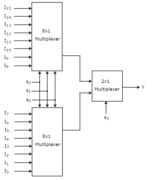
The same selection lines, s2, s1 & s0 are applied to both 8x1 Multiplexers. The data inputs of upper 8x1 Multiplexer are I15 to I8 and the data inputs of lower 8x1 Multiplexer are I7 to I0. Therefore, each 8x1 Multiplexer produces an output based on the values of selection lines, s2, s1 & s0.
The outputs of first stage 8x1 Multiplexers are applied as inputs of 2x1 Multiplexer that is present in second stage. The other selection line, s3 is applied to 2x1 Multiplexer.
- If s3 is zero, then the output of 2x1 Multiplexer will be one of the 8 inputs Is7 to I0 based on the values of selection lines s2, s1 & s0.
- If s3 is one, then the output of 2x1 Multiplexer will be one of the 8 inputs I15 to I8 based on the values of selection lines s2, s1 & s0.
Therefore, the overall combination of two 8x1 Multiplexers and one 2x1 Multiplexer performs as one 16x1 Multiplexer.
AI is thinking...
2. Explain the 4 bit ripple counter and also draw a timing diagram.
A binary ripple counter consists of a series connection of complementing flip-flops (T or JK type), with
the output of each flip-flop connected to the Clock Pulse input of the next higher-order flip-flop. The flip-flop
holding the least significant bit receives the incoming count pulses. The diagram of a 4-bit binary ripple
counter is shown in Fig. below. All J and K inputs are equal to 1.

Fig: 4-bit ripple counter using JK Flip Flop
The small circle in the CP input indicates that the flip-flop complements during a negative-going transition or when the output to which it is connected goes from 1 to 0. The lowest-order bit Q0 must be complemented with each count pulse. Every time Q0 goes from 1 to 0, it complements Q1. Every time Q1 goes from 1 to 0, it complements Q2, and so on.
State Sequence:

Timing Diagram:

In timing diagram Q0 is changing as soon as the negative edge of clock pulse is encountered, Q1 is changing when negative edge of Q0 is encountered(because Q0 is like clock pulse for second flip flop) and so on.
AI is thinking...
3. Design the full subtractor circuit with using Decoder and explain the working principle.
Full subtractor contains 3 inputs and 2 outputs (Difference and Borrow) as shown-

The truth table for full subtractor:

From the above truth table,
For the different functions in the truth table, the minterms can be written as 1,2,4,7, and similarly, for the borrow, the minterms can be written as 1,2,3,7.
Since there are three inputs and a total of eight minterms. So we need 3-to-8 line decoder. The decoder generates the eight minterms for A, B & Bin.
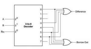
Fig: Full subtractor with 3-to-8 Decoder and NOR gates
AI is thinking...
Short Answer Questions:
AI is thinking...
Attempt any EIGHT questions: (8x5=40)
AI is thinking...
4. Design a half adder logic using only NOR gate.
Input
variables: A & B, Output variables: sum and carry


Logic diagram of half adder using NOR gates only:

AI is thinking...
5. Convert the following decimal numbers into hexadecimal and octal number.
(a) 304 (b) 224
AI is thinking...
6. Describe the three Variable K-map with example.
AI is thinking...
7. Design the Decoder using Universal gates.
AI is thinking...
8. What is combinational logic? What are its important features.
Combinational circuit is a circuit which consist of logic gates whose outputs at any instant of time are determined directly from the present combination of inputs without regard to previous input. The combinational circuit do not use any memory.
There will be combination of input variable for inputs.
A combinational circuit can have number of inputs and number of outputs.
For e.g. adders, subtractors, decoders, encoders etc.

Fig: Block diagram of combinational circuit
AI is thinking...
9. Describe the clocked RS flip-flop.
AI is thinking...
10. What do you mean by triggering of flip flop?
AI is thinking...
11. What are the shift Register operations?
AI is thinking...
12. Describe the Ripple counter.
AI is thinking...
13. Write short notes on:
(a) Registers. (b) Digital. (c) EBCDIC.
AI is thinking...